Frontier Technology
- Published
- Reading time
- 10 minutes
- By
- Como Precision
How 3D Printing Is Entering Quantum and Photonic Hardware
From rewritable quantum light sources to nanoprinted optical surfaces, recent research shows how 3D printing is becoming part of functional photonic hardware.
One of the more consequential directions in 3D printing is easy to miss because the objects are so small. Rather than making a housing around advanced technology, researchers are printing structures that help generate quantum light, transform optical signals, or bring light and atoms into a controlled interaction.
September 2026 developments make that shift worth examining. Paderborn University reported rewritable structures for quantum light sources. Researchers in Shanghai published nanoprinted surfaces for chip-compatible optical transformations. The Ferdinand-Braun-Institut highlighted additive manufacturing within compact atomic quantum sensors, while commercial photonics equipment suppliers emphasized direct printing on fibers and chips.
These are not different announcements of the same technology, and they do not add up to a fully printed quantum computer. Their connection is more interesting: additive manufacturing is becoming a way to engineer functional interfaces inside photonic and quantum hardware. Recent news, read alongside earlier experiments, shows both where that capability is real and where substantial integration work remains.
The printed geometry becomes part of the device
In conventional mechanical applications, a printed part often earns its value through shape, weight, or consolidation. In the examples considered here, geometry can also determine how light is guided, how an optical field is transformed, or how the environment around an atomic experiment is maintained.
The manufacturing methods are not interchangeable. Laser nanoprinting uses photosensitive materials to create very small structures at selected locations. Printed technical ceramics serve a different role, supporting compact, stable assemblies. Patterned vacuum components address another problem again. A desktop polymer printer or a metal powder-bed machine cannot be assumed to reproduce all of these results.
Our synthesis separates four functional roles. The table is a map of the studies discussed below, not a claim that the devices have already been integrated into one system.
| Functional role | What additive manufacturing contributes | Boundary of the demonstrated result |
|---|---|---|
| Quantum light generation | Printed waveguide structures on a lithium niobate platform | A photon-pair source, not a complete quantum processor |
| Optical transformation and coupling | Small diffractive surfaces and precisely positioned micro-optics | Component functions, not a measured replacement for a GPU |
| Temporary optical storage | Hollow structures that guide light through atomic vapor | Weak-pulse storage experiments, not a deployed quantum network |
| Compact atomic instruments | Ceramic optical assemblies and patterned vacuum surfaces | Specific subsystem demonstrations, not universal field qualification |
The useful distinction is therefore not simply “smaller printed parts.” It is whether the manufacturing process gives researchers a new degree of control over the device’s physical function.
Rewritable structures for quantum light sources
Paderborn University’s September 1 announcement describes work with Leibniz University Hannover and Laser Zentrum Hannover on structures made by two-photon polymerization. The team removed printed waveguides from a lithium niobate substrate and printed them again, obtaining comparable performance. This makes the fabrication route potentially useful for revising a device without discarding its entire underlying substrate.
The associated Optics Express research abstract identifies the device more precisely: a printed strip-loaded waveguide on periodically poled thin-film lithium niobate. Photon pairs were generated through spontaneous parametric down-conversion, an optical process that converts a pump photon into two lower-energy photons. The authors report an on-chip pair-generation rate of 4.357 MHz and a coincidence-to-accidental ratio of approximately 404. The latter compares correlated detection events with accidental coincidences; it is not a computing-accuracy score. The on-chip generation rate is also not the rate of useful photons delivered through an entire external system.
The important manufacturing point is what was printed. This is a hybrid structure on an existing optical material platform, not a lithium niobate chip printed from scratch. Likewise, “rewritable” refers here to removing and refabricating structures. It does not mean that a quantum circuit was electronically reprogrammed while operating.
Our interpretation is that this approach changes the cost of a design iteration in principle, even though the cited sources do not quantify a production cost saving. If a functional layer can be revised while retaining the substrate, experimental layouts may become easier to explore. The next question is how consistently that advantage survives repeated fabrication, optical testing, and packaging, rather than whether one successful reprint is possible.
Nanoprinted surfaces for optical computing
A September 16 paper in Advanced Functional Materials approaches the frontier from classical photonics. Researchers at the University of Shanghai for Science and Technology combined physics-driven neural-network design with two-photon nanolithography to make miniature vertical diffractive surfaces. The public abstract reports focusing, beam steering, and orbital-angular-momentum generation, with diffraction efficiencies reaching 91%.
The result concerns shaping optical fields at a scale compatible with photonic chips. In plain terms, the printed geometry redirects and transforms the light itself. It is not merely a holder for a separately manufactured lens. But the reported diffraction efficiency is an optical component metric, not an AI inference accuracy, an electrical efficiency, or evidence that a printed processor outperforms a GPU.
This distinction also separates two uses of AI. A neural-network-based method can help design a physical optical surface; that does not by itself mean the resulting device performs a general neural-network workload. Here, the demonstrated functions are specific transformations of light. Their value for future computing architectures depends on how those functions are combined with sources, detectors, modulation, and the rest of a processing system.
The broader implication, in our analysis, is that fabrication can increasingly encode an optical operation directly into a small structure. That could move some alignment and field-shaping work from a collection of separately positioned components into the manufactured geometry. It does not eliminate the need to measure the resulting optical behavior.
Light cages for temporary optical storage
An earlier study published on January 1, 2026 in Light: Science & Applications demonstrates a different function. Researchers used 3D-nanoprinted hollow waveguides called light cages inside a cesium vapor cell. Their open sides allow atoms to enter the region where light is guided. Multiple structures were integrated on one chip, and attenuated coherent pulses were stored for hundreds of nanoseconds.
This was not a demonstration of a complete quantum repeater or of arbitrary single-photon states stored with high fidelity. The paper discusses further improvements needed for low-noise operation at the single-photon level. Nor were the demonstrated storage times seconds long; those longer times appear in discussion of other memory platforms.
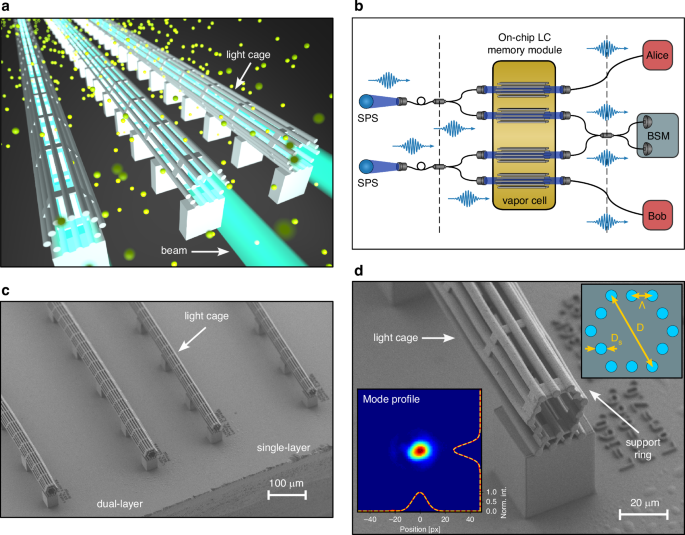
Figure 1 from Gómez-López et al., © The Author(s) 2026, reproduced without modification under CC BY 4.0. Panels a and b are conceptual illustrations; c and d show fabricated structures. The network arrangement in panel b was not demonstrated as a complete network.
The design lesson is that an optical structure may need access to its surroundings, not just isolation from them. A hollow channel with suitable openings can make room for the active medium while controlling the light path. We see this as an example of additive manufacturing enabling an experimental architecture, rather than merely shrinking an existing enclosure.
Ceramics and vacuum structures for compact atomic instruments
Not every useful printed feature directly processes light. Some determine whether a delicate optical experiment can become a compact instrument.
In its September 16 announcement about Marc Christ’s Applied Photonics Award, the Ferdinand-Braun-Institut described a technology platform combining optical micro-integration with printed technical ceramics. The work addresses compact atomic quantum sensors and the material and assembly demands of vacuum and challenging environments. This is recent recognition of an established research program, not evidence that all of its underlying results first appeared in September.
One concrete foundation is the CerAMRef study published in September 2024. Its rubidium optical frequency reference used a printed alumina micro-optical bench and housing. The integrated spectroscopy assembly occupied 6 mL and achieved frequency instability comparable to laboratory setups. The 6 mL figure describes that assembly, not an entire self-contained sensor including all lasers, electronics, and power supplies.
For the manufacturing reader, the point is the relationship between material, geometry, and assembly. A miniature optical bench is useful only if the assembled optics remain where the experiment requires them. The ceramic structure should therefore be understood as part of a precision integration method, not as proof that any printed ceramic can replace a qualified optical assembly.
A January 21, 2026 Physical Review Applied paper adds a less obvious example. Researchers patterned printed vacuum components and applied a non-evaporable getter coating, which captures gas at the surface. They measured gas pumping 3.8 times faster than equivalent flat areas. A possible tenfold improvement was a simulation prediction, not the measured result.
That distinction reveals another functional role for geometry. The printed surface helps determine how residual gas encounters the pumping coating. It is not just a lightweight substitute for a conventional chamber wall. At the same time, a local improvement in surface pumping cannot be translated directly into an identical improvement in sensor accuracy, operating lifetime, or overall vacuum performance.
Photonic packaging is a separate manufacturing milestone
Device research and commercial fabrication equipment are related, but they answer different questions.
On its ECOC 2026 event page for September 21–23, Nanoscribe describes printing freeform micro-optics directly on fibers, photonic chips, and other devices with its Quantum X align platform. The supplier states that fiber cores, chip edges, and other features can be detected to position printed optics, and gives an alignment specification down to 100 nm. Those are manufacturer statements, not an independent production-yield study. The product name does not mean the equipment is itself a quantum computer.
This is significant because a functional optical element still needs to connect to the rest of a system. Positioning it with respect to a real fiber or chip addresses a different problem from producing the same shape on a convenient test substrate. Our reading is that direct, aligned printing could become a bridge between device design and assembly, particularly where interfaces differ in geometry.
The manufacturing milestone to look for is a repeatable packaged optical result. Alignment accuracy alone does not establish insertion loss, temperature stability, durability, or yield after subsequent assembly. Nor does a successful research device prove that a production process can make many equivalent devices economically.
Why these demonstrations do not yet form one machine
It is tempting to arrange the results as a complete chain: generate photons, manipulate them, store them, and integrate the system into a small instrument. That is a useful way to organize the research, but not an experimentally demonstrated architecture assembled from the cited devices.
Before such a combination could work, its components would need compatible wavelengths, optical modes, timing, interfaces, and operating environments. Classical optical field manipulation and quantum-state preservation are also different requirements. A component that performs well in one experiment may need substantial redesign for another.
Loss illustrates the system-level problem without requiring a speculative performance forecast. In a deliberately hypothetical optical path, six successive stages that each transmit 90% of the incoming power would transmit about 53% overall: 0.9 raised to the sixth power is approximately 0.531. This calculation is not a result from the cited studies and is not a quantum-fidelity model. It simply shows why evaluating every component separately can conceal the difficulty of the complete path.
For quantum hardware, the relevant system tests must additionally establish the quality of the quantum states and the effect of noise. For an optical computing device, they must establish the intended computation and its full operating requirements. Printing resolution is an enabling manufacturing characteristic, not a substitute for either kind of validation.
What would mark the next stage of progress
The most useful follow-up results would go beyond a smaller feature or an isolated peak metric. We would look for several fabricated devices behaving consistently, optical performance retained after packaging, and an integrated experiment that measures the benefit of the printed structure against a credible alternative.
For rewritable sources, that means evidence on repeated fabrication and usable output. For printed optical transformations, it means performance in the intended signal-processing path. For memory structures, it means the required storage behavior and noise level together. For compact atomic instruments, it means stable operation under the conditions in which the instrument will actually be used. These are our criteria for interpreting future reports, not claims that every project is pursuing the same application.
For additive manufacturing companies, the opportunity suggested by this research is not necessarily to print an entire quantum machine. It may lie in a specific optical interface, a qualified ceramic assembly, or a functional vacuum component developed with specialists in the relevant physics. None of the cited results transfers automatically to a different printer, material, or supplier.
Taken together, the evidence points to a frontier in which 3D printing contributes more than shape. It can define where light travels, how it is transformed, and how the environment around it is engineered. The likely route forward is hybrid: printed structures working with conventional photonic materials, coatings, optics, and electronics. That is a more demanding role than making a prototype enclosure, and a more precise account of the progress than saying that quantum computers can now be printed.
Sources and disclosure
Public information reviewed for this article
This article is an original Como Precision analysis based on public online information from the sources listed below. Research findings apply to the devices and conditions studied; institutional news and supplier specifications are attributed to their issuers. The photon-pair source, diffractive neural surfaces, and patterned vacuum surface results were checked against publicly accessible research abstracts, not independently reproduced experiments. Earlier studies are dated in the text. The comparison and illustrative loss calculation are our analysis. The reproduced research figure is credited separately under its Creative Commons license. These reports do not establish Como Precision capability in quantum or photonic device manufacturing.
- Rewritable light sources for quantum technologies produced using a 3D printer Paderborn University · Accessed Oct 3, 2026
- High-performance photon-pair source using a two-photon-polymerized strip-loaded lithium niobate waveguide Optics Express via Paderborn University Research Information System · Accessed Oct 3, 2026
- Chip-Compatible Optical Field Manipulation for a Single Mode Fiber Using Ultrathin 3D-Nanoprinted Diffractive Neural Surfaces Advanced Functional Materials · Accessed Oct 3, 2026
- Light storage in light cages: a scalable platform for multiplexed quantum memories Light: Science & Applications · Accessed Oct 3, 2026
- Marc Christ receives Applied Photonics Award 2026 for his dissertation on compact atomic quantum sensors Ferdinand-Braun-Institut · Accessed Oct 3, 2026
- Additively Manufactured Ceramics for Compact Quantum Technologies Advanced Quantum Technologies · Accessed Oct 3, 2026
- Exploiting complex 3D-printed surface structures for portable quantum technologies Physical Review Applied · Accessed Oct 3, 2026
- ECOC 2026 Nanoscribe · Accessed Oct 3, 2026
Project review
Send drawings, material requirements, quantities, and acceptance criteria for a scoped technical review.
Contact Como